Logic Circuits
(Content adapted from Critchlow & Eck)
Gates
Computers have a reputation—not always deserved—for being "logical." But fundamentally, deep down, they are made of logic in a very real sense. The building blocks of computers are logic gates, which are electronic components that compute the values of simple propositions such as and . (Each gate is in turn built of even smaller electronic components called transistors; we will explore this briefly below.)
A wire in a computer can be in one of two states, which we can think of as being on and off. These two states can be naturally associated with the Boolean values and . When a computer computes, the multitude of wires inside it are turned on and off in patterns that are determined by certain rules. The rules involved can be most naturally expressed in terms of logic. A simple rule might be, "turn wire on whenever wire is on and wire is on." This rule can be implemented in hardware as an AND gate. An AND gate is an electronic component with two input wires and one output wire, whose job is to turn its output on when both of its inputs are on and to turn its output off in any other case. If we associate "on" with and "off" with , and if we give the names and to the inputs of the gate, then the gate computes the value of the logical expression . In effect, is a proposition with the meaning "the first input is on," and is a proposition with the meaning "the second input is on." The AND gate functions to ensure that the output is described by the proposition . That is, the output is on if and only if the first input is on and the second input is on.
An OR gate is an electronic component with two inputs and one output which turns its output on if either (or both) of its inputs is on. If the inputs are given names and , then the OR gate computes the logical value of . A NOT gate has one input and one output, and it turns its output off when the input is on and on when the input is off. If the input is named , then the NOT gate computes the value of .
Other types of logic gates are, of course, possible. Gates could be made to compute or , for example. However, any computation that can be performed by logic gates can be done using only AND, OR, and NOT gates, as we will see below. (In practice, however, NAND gates and NOR gates, which compute the values of and respectively, are often used because they are easier to build from transistors than AND and OR gates.)
The three types of logic gates are represented by standard symbols, as shown in the figure below. Since the inputs and outputs of logic gates are just wires carrying on/off signals, logic gates can be wired together by connecting outputs from some gates to inputs of other gates. The result is a logic circuit. The figure also shows an example circuit that computes the value of the logical expression . The input wires to each logic gate are on the left, with the output wire on the right. Note that when wires cross each other in a diagram such as this, the wires don't actually intersect unless there is a black circle at the point where they cross.
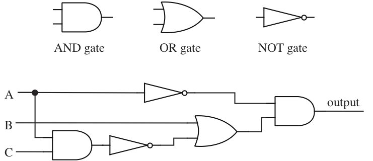
The logic circuit in the figure has three inputs, labeled , , and . The circuit computes the value of the compound proposition . That is, when represents the proposition "the input wire labeled is on," and similarly for and , then the output of the circuit is on if and only if the value of the compound proposition is true.
Here is a tool where you can play with the above circuit:
Constructing Gates from Transistors
It is useful to have some idea of how digital logic gates are built out of lower-level electronic devices such as transistors. For our purposes, a transistor is a voltage-controlled switch: when the controlling voltage is high, the switch is closed (that is, it conducts electricity); when the controlling voltage is low, the switch is open (breaking the connection). The figure below shows n-type metal-oxide-semiconductor (NMOS) implementations of NOT, NOR, and NAND gates; we will study these instead of the more common complementary MOS (CMOS) gates, because they are slightly simpler---CMOS has the practical advantage of using significantly less power, at the cost of doubling the number of transistors, but the basic principles are very similar.

The NOT gate consists of a single transistor in the lower half: the gate on the left is connected to the input signal, ; the source at the bottom is connected to ground (0), and the drain at the top is connected to the output, , and a pull-up resistor (the jagged line) whose other end is at the high voltage level (1). When and the switch is open (so the transistor effectively has infinite resistance), the output will be pulled high (so ). When and the switch is closed, the lower resistance through the transistor will pull the output low (so ).
The NOR gate uses two transistors in parallel: if either or is high, then the output () will be pulled low. Conversely, the NAND gate uses two transistors in series: both have to be closed (so ) for the output () to be pulled to 0. The next figure shows the conventional circuit symbols for NAND and NOR gates (note that the circle on the output indicates negation, just like on the NOT gate; the unnegated version of NOT, drawn as a simple triangle, is known as a buffer, because it copies its input to its output unchanged, after a short delay).

Those three gates are the simplest to implement with transistors. As we saw in the exercises in the Propositional Logic section, all other Boolean operators can be constructed from NAND alone, or NOR alone. For example, an AND gate is a NAND followed by a NOT, so it can be built out of three transistors;1 an OR gate also takes three, using a NOR and a NOT. In the Circuit Simplification section, we will see another way to construct circuits using only NAND gates.
Building a Circuit from a Proposition
Given any compound proposition made from the operators , , and , it is possible to build a logic circuit that computes the value of that proposition. The proposition itself is a blueprint for the circuit. As noted in the Propositional Logic section, every logical operator that we have encountered can be expressed in terms of , , and , so in fact every compound proposition that we know how to write can be computed by a logic circuit.
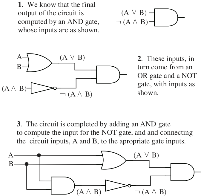
Given a proposition constructed from , , and operators, it is easy to build a circuit to compute it. First, identify the main operator in the proposition—the one whose value will be computed last. Consider . This circuit has two input values, and , which are represented by wires coming into the circuit. The circuit has an output wire that represents the computed value of the proposition. The main operator in , is the first , which computes the value of the expression as a whole by combining the values of the subexpressions and . This operator corresponds to an AND gate in the circuit that computes the final output of the circuit.
Once the main operator has been identified and represented as a logic gate, you just have to build circuits to compute the input or inputs to that operator. In the example, the inputs to the main AND gate come from two subcircuits. One subcircuit computes the value of and the other computes the value of . Building each subcircuit is a separate problem, but smaller than the problem you started with. Eventually, you'll come to a gate whose input comes directly from one of the input wires— or in this case—instead of from a subcircuit.
Here is the resulting circuit in CircuitVerse:
Circuits as Expression Trees
A combinational circuit is one in which the output is entirely determined by the inputs—it is a pure function, with no dependence on state or time (apart from the initial time it takes the circuit to compute the output; we will discuss this more in the next section). As such, its behavior is completely determined by a truth table; as we have seen, this means that it corresponds to a logical expression built up from the inputs and our basic operators.
When implementing a Boolean expression as a digital circuit, it is conventional to use a two-dimensional graphical representation of the circuit. This is partly because the circuit will eventually be laid out on a physical circuit board or semiconductor chip, and the relative locations of the gates and their interconnections will be important (although we will not go to this level of detail), but also because it can be easier to examine some of the properties and behavior of a circuit in a graphical form.
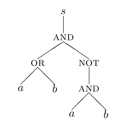
Another way to get this graphical representation is to use an expression tree, which is a variation of the parse trees studied later in the course. For example, we may picture the expression as the following:
Of course, we are usually interested in circuits that may have multiple outputs, so we may use a forest of expression trees. The next figure shows a forest for the same expression as above, along with the additional output given by :
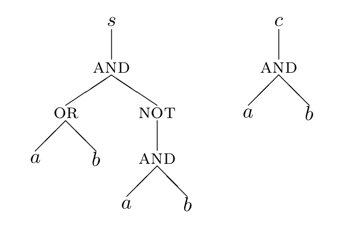
Upon doing this, we might notice that the subtree for is duplicated. It would be nice to share common parts of the circuit, thus giving us an expression DAG (directed acyclic graph) instead of a tree or forest. One way to do this is shown next:
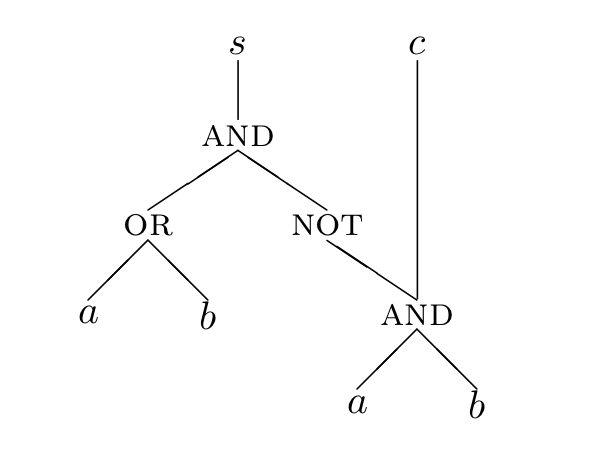
We could also share the inputs rather than repeating them, as shown next; this is still a DAG:

Finally, instead of using the words AND, OR, and NOT, we will use the corresponding circuit symbols; we also draw the DAG "on its side," so that the flow from inputs to outputs is left-to-right. The final result is a circuit diagram such as this:

It is important to realize, though, that this is just another presentation of the logical expressions we started with. Any set of Boolean expressions may be drawn this way, and any circuit where all of the information flows from left to right may be read as a set of expressions.
In addition to visualizing the layout of gates in a digital circuit, a circuit diagram may be used to "trace" its operation on particular inputs. For example, the diagram below shows our example circuit annotated with 0/1 logic values on each wire, to trace its behavior when both inputs and are 1. Since the logic values flow from left to right, the output of each successive gate may be determined from its inputs. By tracing each combination of inputs, we may construct a truth table corresponding to the circuit; the result is
| 0 | 0 | 0 | 0 |
| 0 | 1 | 0 | 1 |
| 1 | 0 | 0 | 1 |
| 1 | 1 | 1 | 0 |

The CircuitVerse simulator can also be used to interactively trace the behavior of a circuit. Click on the inputs (A and B) in the circuit to see the effect on the outputs. Wires with a 1 value show up as bright green.
Extracting a Proposition from a Combinational Circuit
So, every compound proposition is computed by a logic circuit with one output wire. Is the reverse true? That is, given a logic circuit with one output, is there a proposition that expresses the value of the output in terms of the values of the inputs? Not quite. When you wire together some logic gates to make a circuit, there is nothing to stop you from introducing feedback loops. A feedback loop occurs when the output from a gate is connected—possibly through one or more intermediate gates—back to an input of the same gate. Here is an example of a circuit with a feedback loop:
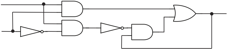
The feedback loop includes the AND gate and the OR gate on the right. This circuit does not compute the value of a compound proposition. This circuit does, however, play an important role in computer memories, since it can be used to store a logical value.
Here is that circuit in CircuitVerse. Leaving X at 0, choose a value for Y (either 0 or 1). Now toggle X to 1 and back to 0, and observe that Z remembers the chosen value of Y for as long as X remains 0, even if you change the Y input.
Feedback loops cannot be described by compound propositions, basically because there is no place to start, no input to associate with a propositional variable. But feedback loops are really the only thing that can go wrong when trying to describe a circuit with propositional logic. A logic circuit that does not contain any feedback loops is called a combinational logic circuit, because the output is determined solely by the combination of values on the inputs.2 Every combinational logic circuit with just one output computes the value of some compound proposition. The propositional variables in the compound proposition are just names associated with the input wires of the circuit. (Of course, if the circuit has more than one output, you can simply use a different proposition for each output.)
The key to understanding why this is true is to note that each wire in the circuit—not just the final output wire—represents the value of some proposition. Furthermore, once you know which proposition is represented by each input wire to a gate, it's obvious what proposition is represented by the output: You just combine the input propositions with the appropriate , , or operator, depending on what type of gate it is. To find the proposition associated with the final output, you just have to start from the inputs and move through the circuit, labeling the output wire of each gate with the proposition that it represents. This figure illustrates the process:
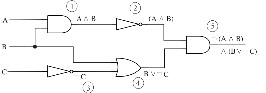
Each wire in the circuit is labeled with the proposition that it represents. The numbering of the labels shows one of the orders in which they can be associated with the wires. The circuit as a whole computes the value of .
Once more, here is the same circuit in CircuitVerse:
Disjunctive Normal Form
So, compound propositions correspond naturally with combinational logic circuits. But we have still not quite settled the question of just how powerful these circuits and propositions are. We've looked at a number of logical operators and noted that they can all be expressed in terms of , , and . But might there be other operators that cannot be so expressed? Equivalently, might there be other types of logic gates—possibly with some large number of inputs—whose computations cannot be duplicated with AND, OR, and NOT gates? Any logical operator or logic gate computes a value for each possible combination of logical values of its inputs. We could always make a truth table showing the output for each possible combination of inputs. As it turns out, given any such truth table, it is possible to find a proposition, containing only the , , and operators, whose value for each combination of inputs is given precisely by that table.
To see why this is true, it is useful to introduce a particular type of compound proposition. Define a simple term to be either a propositional variable or the negation of a propositional variable. A conjunction of simple terms would then consist of one or more simple terms put together with operators. (A "conjunction of one simple term" is just a single simple term by itself. This might not make grammatical sense, but it's the way mathematicians think.) Some examples of conjunctions of simple terms would be , , , and . Finally, we can take one or more such conjunctions and join them into a "disjunction of conjunctions of simple terms." This is the type of compound proposition we need. We can avoid some redundancy by assuming that no propositional variable occurs more than once in a single conjunction (since can be replaced by , and if and both occur in a conjunction, then the value of the conjuction is false, and it can be eliminated.) We can also assume that the same conjunction does not occur twice in the disjunction.
A compound proposition is said to be in disjunctive normal form, or DNF, if it is a disjunction of conjunctions of simple terms, and if, furthermore, each propositional variable occurs at most once in each conjunction and each conjunction occurs at most once in the disjunction.
Using , , , , , and as propositional variables, here are a few examples of propositions that are in disjunctive normal form:
Propositions in DNF are just what we need to deal with input/output tables of the type that we have been discussing. Any such table can be computed by a proposition in disjunctive normal form. It follows that it is possible to build a circuit to compute that table using only AND, OR, and NOT gates.
Theorem: DNF
Consider a table that lists a logical output value for every combination of values of several propositional variables. Assume that at least one of the output values is true. Then there is a proposition containing those variables such that the value of the proposition for each possible combination of the values of the variables is precisely the value specified in the table. It is possible to choose the proposition to be in disjunctive normal form.
Proof:
Consider any row in the table for which the output value is . Form a conjunction of simple terms as follows: For each variable, , whose value is in that row, include itself in the conjunction; for each variable, , whose value is in the row, include in the conjunction. The value of this conjunction is for the combination of variable values given in that row of the table, since each of the simple terms in the conjuction is true for that combination of variables. Furthermore, for any other possible combination of variable values, the value of the conjunction will be , since at least one of the simple terms in the conjunction will be false.
Take the disjunction of all such conjunctions constructed in this way, for each row in the table where the output value is true. This disjunction has the value if and only if one of the conjunctions that make it up has the value —and that is precisely when the output value specified by the table is . So, this disjunction of conjunctions satisfies the requirements of the theorem.
As an example, consider the table below. This table specifies a desired output value for each possible combination of values for the propositional variables , , and . Look at the second row of the table, where the output value is true. According to the proof of the theorem, this row corresponds to the conjunction . This conjunction is true when is false, is false, and is true; in all other cases it is false, since in any other case at least one of the terms , , or is false. The other two rows where the output is true give two more conjunctions. The three conjunctions are combined to produce the DNF proposition . This proposition computes all the output values specified in the table. Using this proposition as a blueprint, we get a logic circuit whose outputs match those given in the table (see below).
| output | conjunction | |||
|---|---|---|---|---|
Equivalent Circuits
Now, given any combinational logic circuit, there are many other circuits that have the same input/output behavior. When two circuits have the same input/output table, the compound propositions associated with the two circuits are logically equivalent. To put this another way, propositions that are logically equivalent produce circuits that have the same input/output behavior. As a practical matter, we will usually prefer the circuit that is simpler. The correspondence between circuits and propositions allows us to apply Boolean algebra to the simplification of circuits.
For example, consider the DNF proposition corresponding to the table above. In , we can factor from the last two terms, giving . Since , and for any proposition , this can be simplified to . Again, we can apply the distributive law to this to factor out an , giving . One more application of the distributive law will turn this into , which further simplifies to . This compound proposition is logically equivalent to the one we started with, but implementing it in a circuit requires only three logic gates, instead of the ten required by the original proposition.3
Here are three versions (select the "tabs" in the upper-left) of circuits implementing this truth table in CircuitVerse:
The "DNF" tab is the direct implementation of the DNF expression, using three-input AND and OR gates. The "DNF-2Input" tab is the same circuit using only two-input gates. The "Simplified" tab is the final equivalent circuit. You should check that all three have the same truth table behavior.
If you start with a circuit instead of a proposition, it is often possible to find the associated proposition, simplify it using Boolean algebra, and use the simplified proposition to build an equivalent circuit that is simpler than the original.
Binary Arithmetic
All this explains nicely the relationship between logic and circuits, but it doesn't explain why logic circuits should be used in computers in the first place. Part of the explanation is found in the fact that computers use binary numbers. A binary number is a string of zeros and ones. Binary numbers are easy to represent in an electronic device like a computer: Each position in the number corresponds to a wire. When the wire is on, it represents one; when the wire is off, it represents zero. When we are thinking in terms of logic, the same states of the wire represent true and false, but either representation is just an interpretation of the reality, which is a wire that is on or off. The question is whether the interpretation is fruitful.
Once wires are thought of as representing zeros and ones, we can build circuits to do computations with binary numbers. Which computations? Any that we want! If we know what the answer should be for each combination of inputs, then by the DNF Theorem we can build a circuit to compute that answer. Of course, the procedure described in that theorem is only practical for small circuits, but small circuits can be used as building blocks to make all the calculating circuits in a computer.
For example, let's look at binary addition. To add two ordinary, decimal numbers, you line them up one on top of the other, and add the digits in each column. In each column, there might also be a carry from the previous column. To add up a column, you only need to remember a small number of rules, such as and . For binary addition, it's even easier, since the only digits are 0 and 1. There are only eight rules:
Here, I've written each sum using two digits. In a multi-column addition, one of these digits is carried over to the next column. Here, we have a calculation that has three inputs and two outputs. We can make an input/output table for each of the two outputs. The table is shown below. We know that the outputs in this table can be implemented as combinational circuits, so we know that circuits can add binary numbers. To add multi-digit binary numbers, we just need one copy of the basic addition circuit for each column in the sum.
| carry output | sum output | |||
|---|---|---|---|---|
| 0 | 0 | 0 | 0 | 0 |
| 0 | 0 | 1 | 0 | 1 |
| 0 | 1 | 0 | 0 | 1 |
| 0 | 1 | 1 | 1 | 0 |
| 1 | 0 | 0 | 0 | 1 |
| 1 | 0 | 1 | 1 | 0 |
| 1 | 1 | 0 | 1 | 0 |
| 1 | 1 | 1 | 1 | 1 |
Exercises
Using only AND, OR, and NOT gates, draw circuits that compute the value of each of the propositions , , and .
Answer
The circuits may easily be drawn from the expressions:
Other solutions are possible.
For each of the following propositions, find a combinational logic circuit that computes that proposition:
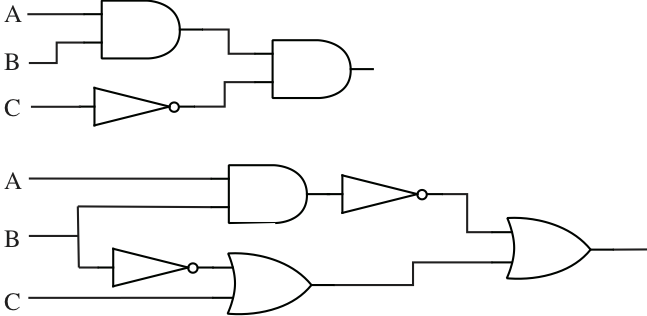
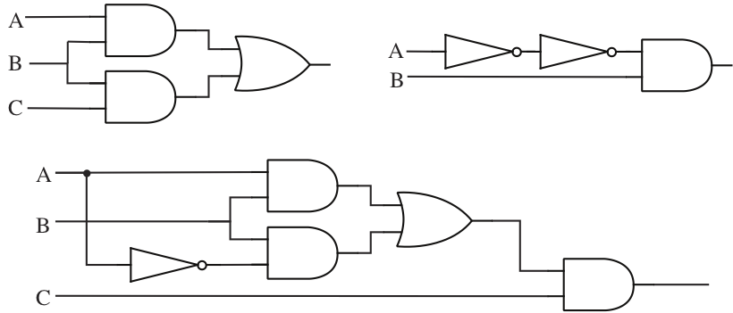
Find the compound proposition computed by each of the following circuits:
Answer
The first is , and the second is .
This section describes a method for finding the compound proposition computed by any combinational logic circuit. This method fails if you try to apply it to a circuit that contains a feedback loop. What goes wrong? Give an example.
Answer
When there is a loop, it is not possible to give expressions for all the inputs of a gate in the loop until you know an expression for its output. For example, suppose we have a loop where the output of an OR feeds one input of an AND, which in turn feeds back to one of the inputs of the OR. We do not have an expression for both of the inputs to the OR until we have an expression for the output of the AND, which depends on knowing an expression for the output of the OR.
Show that every compound proposition which is not a contradiction is equivalent to a proposition in disjunctive normal form. (Note: We can eliminate the restriction that the compound proposition is not a contradiction by agreeing that "" counts as a proposition in disjunctive normal form. is logically equivalent to any contradiction.)
Answer
This follows directly from the proof of the DNF theorem, since if a proposition is not a contradiction then at least one of the rows of its truth tables must be true.
A proposition in conjunctive normal form (CNF) is a conjunction of disjunctions of simple terms (with the proviso, as in the definition of DNF, that a single item also counts as a disjunction). Show that every compound proposition which is not a tautology is logically equivalent to a compound proposition in conjunctive normal form. (Hint: What happens if you take the negation of a DNF proposition and apply De Morgan's Laws?)
Answer
Given a proposition that is not a tautology, its negation will be a propostion that is not a contradiction. As in the previous exercise, the DNF theorem allows us to construct a DNF expression that is equivalent to the negation of the original proposition. Taking the negation of this DNF expression (which will give us a result that is equivalent to the original proposition) and applying De Morgan's laws, will turn the disjunction of some conjunctions of simple terms into the conjunction of some disjunctions of negated simple terms. Finally, a negated simple term is equivalent to a simple term, because if it was already a negated variable then we can use the double-negation law to turn it into a plain variable.
Use the laws of Boolean algebra to simplify each of the following circuits:
Answer
- Design circuits to implement the input/output tables
for addition, as given in the section above. Try to
make your circuits as simple as possible. (The circuits that are
used in real computers for this purpose are more simplified than
the ones you will probably come up with, but the general approach
of using logic to design computer circuits is valid.)
Answer
For one approach, see the full adder circuit in Common Circuit Components.
- A NOT gate may be thought of as a degenerate, single-input version of either NAND or NOR, which requires only a single transistor in NMOS.↩
- By contrast, a circuit with a feedback loop is called a sequential logic circuit, because the behavior of the circuit depends on the exact sequence of when input signals change.↩
- No, I didn't count wrong. There are eleven logical operators in the original expression, but you can get by with ten gates in the circuit: Use a single NOT gate to compute , and connect the output of that gate to two different AND gates. Reusing the output of a logic gate is an obvious way to simplify circuits that does not correspond to any operation on propositions.↩